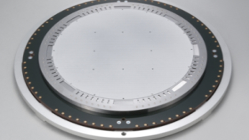
Components for Semiconductor Inspection Equipment (Contact Probe Related Products)

Inspection Characteristics

Fine pitch

109狭ピッチ

Fine Pitch Unit

It mainly refers to a pitch of 200μm or less, and is used for inspection fixtures for wafer testing before semiconductor assembly. The probe tip position and protrusion amount must be accurate, and high technology is required for designing and manufacturing. NHK Spring manufactures Probe Head supporting probes.

RF

Electromagnetic field analysis application (ANSYS HFSS)

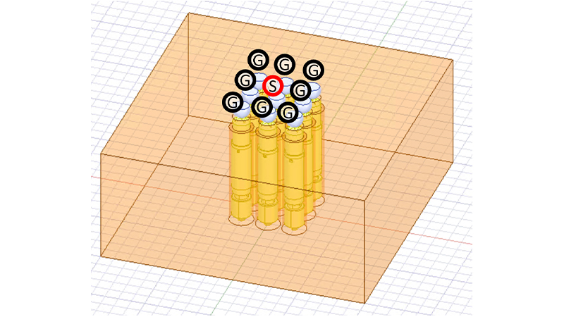
Ex) Multi-pin analysis model

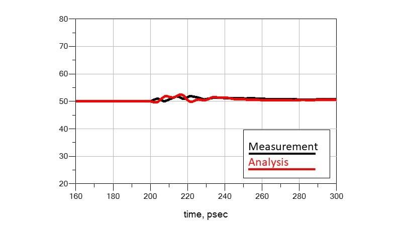
Insertion Loss (S21)
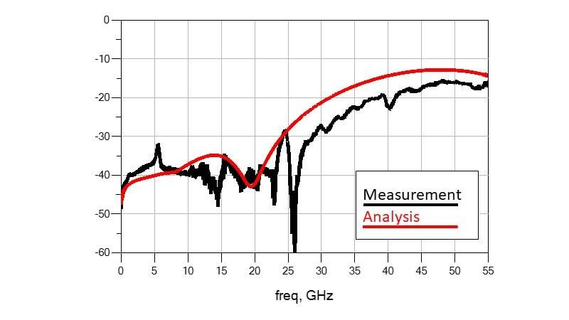
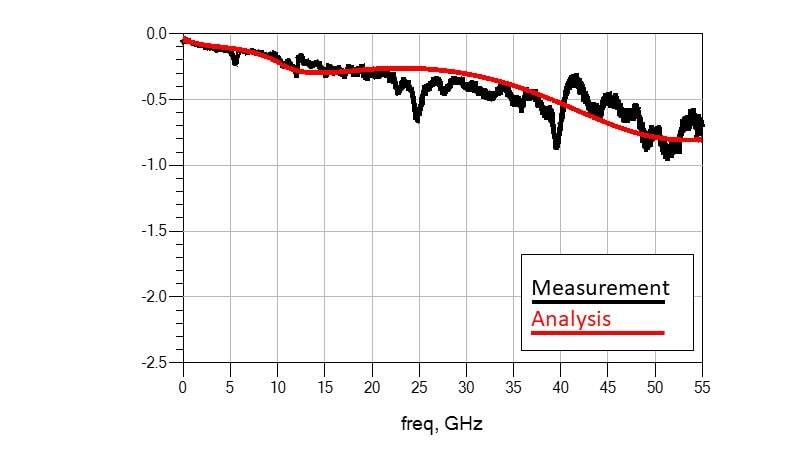
Return Loss (S11)

TDR

In RF measurement above 20 GHz, the influence of the measurement fixture cannot be ignored, so we have developed a dedicated measurement fixture in-house to minimize the influence.The results of actual measurement and analysis are consistent and highly reputed by our customers.

We can also send you the actual and simulated Touch stone file (.sNp) so that you can check the waveform and Eye-Pattern when connected to your devices.

We basically measure and analyze GND-Signal-GND arrays, but we can also flexibly conduct multi-pin and X-talk analysis according to customer requests.

Since the probe is affected by devices, it is important to be matched to customer PCB impedance. We can get the information of the PCB from the customer and bring the impedance of the probe closer, so please consult with us.